Loop Antenna
Loop Antenna
This design is inspired by Wellbrook's ALA1530LN, which is considered one of the best loop antennas available. Our design further enhances the original to reduce noise and improve performance.
The design strategically utilizes 8 JFETs (Junction Field Effect Transistors) to minimize the noise figure, which is crucial for enhancing overall signal quality and achieving high performance in sensitive applications. JFETs were chosen for their low noise characteristics and high input impedance, making them ideal for applications requiring minimal signal degradation.
In our laboratory tests, the design yielded the following performance results:
OIP3 (Output Third-Order Intercept Point): 44.1 dB. This parameter is a measure of the linearity of the system and indicates how well the design handles high signal levels without introducing significant distortion. A higher OIP3 value reflects better performance in maintaining signal integrity under high input conditions.
Input Impedance Measurements: The input impedance of the system was evaluated at various frequencies:
- At 170 kHz, the input impedance was 24 ohms.
- At 9 MHz, the input impedance was 21 ohms.
- At 24 MHz, the input impedance increased to 69 ohms.
- At 33 MHz, the impedance further increased to 169.6 ohms.
These measurements highlight how the input impedance of the system varies with frequency, which is an important aspect of impedance matching and overall system performance. The varying impedance at different frequencies must be considered to ensure optimal operation and integration with other components in the circuit.
SPICE model
SPICE model can be download here as Zip Package.
This model is based on John VE6EY Wideband Magnetic Loop Model implemented in LTSpice. Please install LTSpice to view and play with the model.
Build
In addition to the PCB, you will need a suitable enclosure to securely house the circuit board. This enclosure will protect the PCB from physical damage and environmental factors. Additionally, a metal loop is required, preferably made of aluminum, which is lightweight and durable. The loop should have a diameter of approximately 1 meter. This metal loop must be connected to the designated "LOOP" connection point on the PCB to ensure proper functionality. Make sure the connection is secure and aligned with the system's requirements for optimal performance.
Schematic & BOM
Schematic can be downloaded here as PDF
| ID | Quantity | Name | Model | Package | Description |
|---|---|---|---|---|---|
| 1 | 2 | Q19 Q21 | Transistor 2N4401 | Through-hole | ON Semiconductor may be better |
| 2 | 8 | Q11-18 | JFET 2SK715V | Through-hole | |
| 3 | 4 | C1-2 C25 C29 | Ceramic Capacitor 100nF | R0805 | |
| 4 | 4 | C26 C8 C32-33 | Ceramic Capacitor 100nF | R0603 | |
| 5 | 1 | C6 | Ceramic Capacitor 10pF | R0603 | |
| 6 | 5 | C3 C7 C10 C15 C31 | Ceramic Capacitor 2.2uF | R0805 | |
| 7 | 2 | C4-5 | Ceramic Capacitor 82pF | R0603 | |
| 8 | 1 | C73 | Surface-Mount Solid Capacitor D=8 100uF/16V | E_E7 | |
| 9 | 2 | J1-2 | Diode 1N60P | Through-hole | |
| 10 | 4 | D1-4 | Dual Diode BAV99 | SOT23 | |
| 11 | 1 | LA1 | Power Inductor 1mH | IND-7X7 | |
| 12 | 2 | L2-3 | Ferrite Bead 220R@100M | R0805 | |
| 13 | 1 | RA1 | Surface-Mount Resistor 1.2K | R0805 | |
| 14 | 1 | RA7 | Surface-Mount Resistor 2.7k | R0805 | |
| 15 | 1 | RA2 | Surface-Mount Resistor 510R | R0805 | |
| 16 | 2 | RA3 RA6 | Surface-Mount Resistor 51R | R0805 | |
| 17 | 1 | T1 | Hand-wound Balun | BN73-302 | |
| 18 | 1 | T2 | Hand-wound Balun | BN73-302 | |
| 19 | 1 | R1 | Precision Adjustable Resistor 100R | 67YR100R | Can be omitted; change RA3 RA6 to 24R |
Transformers Wound Instructions
T1
Start by making some double wires; you can twist together two enameled copper wires. It's often helpful to use two different colors of wire or to color one of the wires in the twisted pair with a permanent marker. If you can't color the wires, it's easy to sort them after winding using an ohmmeter. Use enameled copper wire with a diameter of 0.25 mm, or wire with a diameter of 0.2 mm.
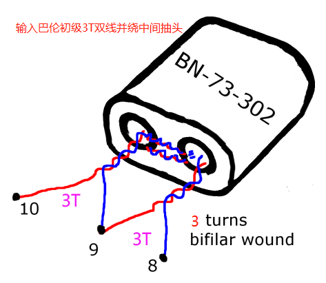
The first task is to wind the loop (input) side of T1. Wind 3 turns of double wire around the BN-73-302 core to form a center tap point, as shown.
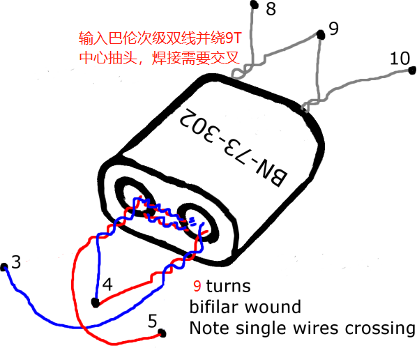
Flip the core and repeat the process to create the first secondary winding of T1. Like the primary, the two wires are joined together to form a center tap and will be connected to pin 4. The remaining two wires need to cross each other to prevent circuit oscillation.
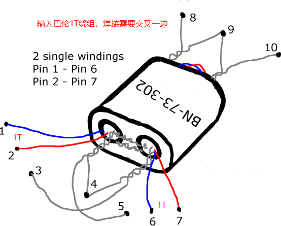
At this point, it may be easier to mount the T1 transformer on the PCB and then add the two single-turn windings— for a binocular core, a turn is a “U” loop through two holes. The final two windings are made with a single wire (not double wire), entering from one side of the core and exiting from the other. One winding connects from pin 1 to pin 6, and the other winding connects from pin 2 to pin 7, as shown.
By this time, you should have installed the T1 transformer correctly. If your build encounters high-frequency oscillation (15-30MHz), adding an extra feedback loop, i.e., taking the ends 6 and 7 through the core to end at the same point, usually helps. This situation occasionally occurs when the transistor has an unusually high hfe.
T2
Use the same double wire as for T1 to wind 9 turns of the primary for transformer T2. Separate the two wires and create the center tap as before, as shown. Like T1, you can use enameled copper wire with a diameter of 0.25 mm or wire with a diameter of 0.2 mm.
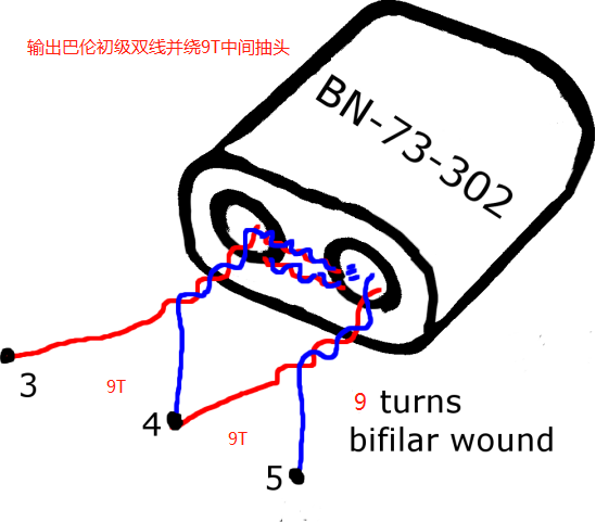
The secondary winding for T2 is 6 turns of standard (single-core) enameled copper wire, as shown.
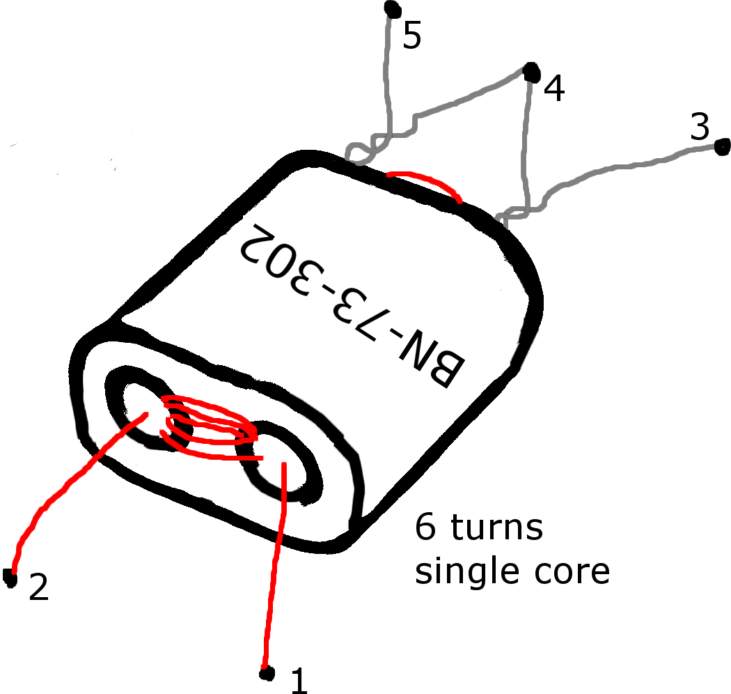
Mount it on the PCB, and transformer T2 is now completed.
Gerber Files
The design for rectangle PCB: Gerber File
The design for circle PCB: Gerber File
Tips
How to use Gerber file to order PCB from JLC, please refer the document here: Instruction