FPGA Design
FPGA Design
This article provides a high-level overview of the Web-888 FPGA implementation.
Overview
The Zynq-7010 features a unique combination of a high-performance CPU core and a reasonably sized FPGA. Multiple buses connect these two components, allowing us to leverage this architecture for the implementation of Web-888.
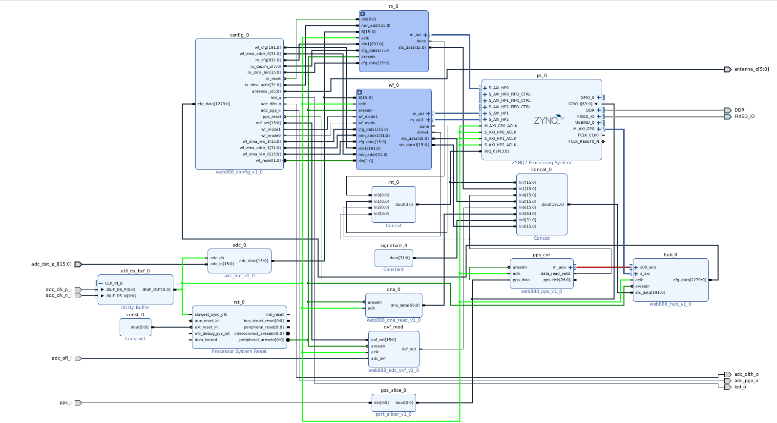
The FPGA implementation uses Vivado block design. At a high level, the design includes several important building blocks. Most blocks are create from scratch with some building blocks are coming from Xilinx like CIC filters.
RX block This block connects to the generic memory port of the ARM CPU and supports RX channels. The data rate from this module to the CPU is 16 bits * 2 (IQ) * 13 channels * 12K = 4.992Mbps.
WF Block This block connects to two high-performance memory ports of the ARM CPU. Each channel serves one WF sampling channel. The data rate from this module to the CPU is 3.9Gbps when in Zoom0 mode of a WF.
Config Block + Hub Block These two blocks manage all the configurations for the RX and WF channels, exposing the configurations to the ARM CPU.
pps_cnt block This block uses the FPGA to count clock pulses in one PPS (Pulse Per Second) cycle, measuring clock accuracy via GPS.
Note
The diagram is exported via the Vivado block designer. It may change during development or bug fixes.
Resource Usage
Zynq-7010 already uses about 80% of the FPGA resource while we still be able to manage the timing. 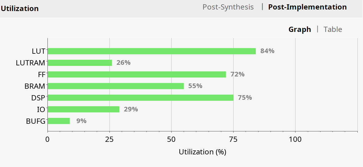
We are running FPGA at 122.88Mhz. The following timing is still sufficient to support this frequency. 
RX Block
The RX block must support 13 RX channels. We use a two-level CIC filter to decimate the IQ data to 12K. Since the data rate is fixed and not very high, we chose to use the General Purpose port of the CPU to pass the data. A simple DMA is implemented to continuously transfer the data to the CPU.
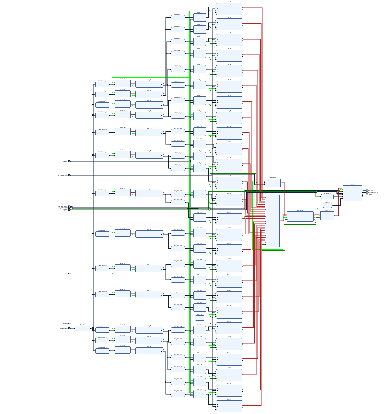
The diagram is densely packed since we have 26 data paths in the RX block. Let's focus on one path to understand the details.
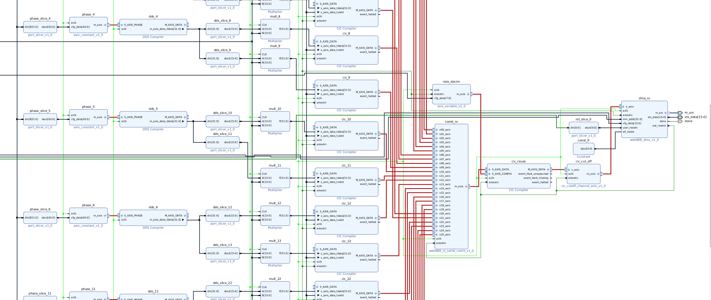
From left to right, the ADC data passes through multiple stages. The first stage is a DDC (Digital Down Converter). Technically, this converter consists of two multipliers and one DDS. The DDS outputs sine and cosine data to convert ADC data from real to complex (IQ data) and simultaneously move it to the baseband. Both I and Q then pass through a 3-stage CIC filter (d=256) to decimate the data to 480K. To save FPGA resources, we combine all 26 channels into one stream (with some padding) and pass it through a 5-stage single CIC filter (d=40) to decimate the data to 12K. The rightmost part shows a DMA block that transfers the data to the CPU.
We are using CIC filter from Xilinx, which has the ability to support multi channels. It is the secret sauce to support 13 channels.
To maintain SNR, the data uses 32 bits per sample. The DDC multiplies 16-bit ADC data with 16-bit DDS data to produce 32-bit output. We can pass 32-bit I and 32-bit Q data to the CPU thanks to the fast interconnection between the CPU and FPGA.
WF Block
The WF block supports two channels. These two channels can be time-multiplexed by the software to support WF for all 13 channels. The WF has different performance requirements than the RX since it can sample at the ADC clock rate of 122.88 MHz. Therefore, we dedicate resources to both channels without any shared resources like the RX block.
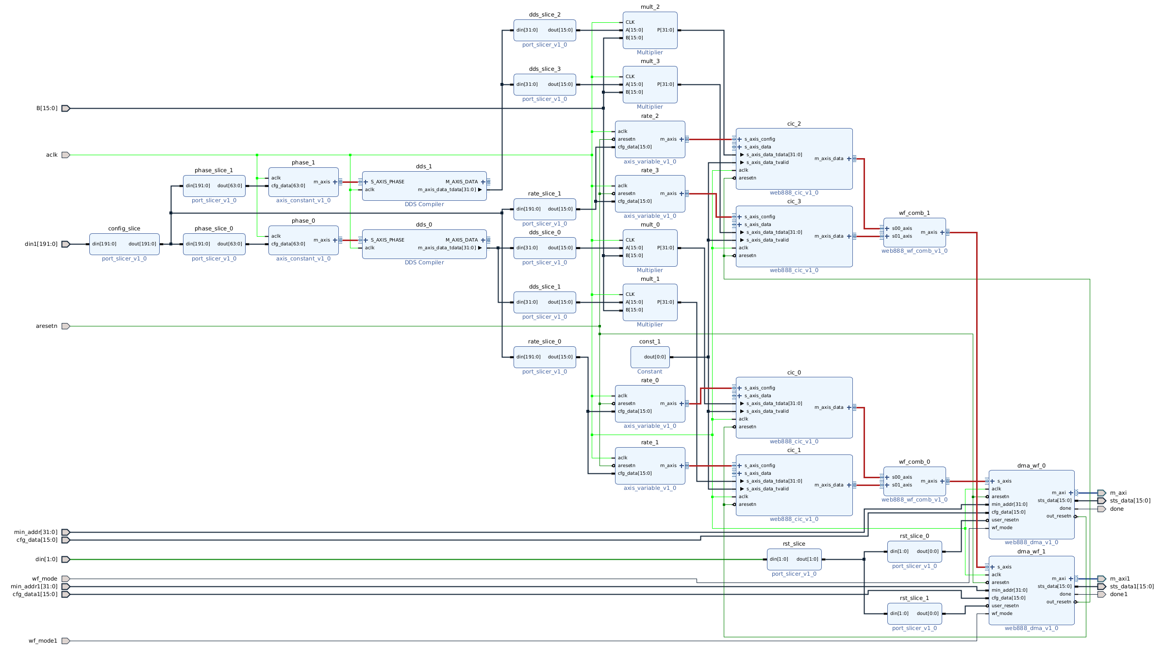
From left to right, the ADC data path is similar to that of the RX channel but with some differences:
- The WF block uses only one 5-stage CIC filter. Due to FPGA resource constraints, we limit this to a single-stage CIC filter here.
- The WF CIC output data is 16 bits, compared to the 32-bit output in the RX block. Since the WF data is ultimately mapped to a 256-color scale for presentation, 16 bits of data are more than sufficient.
- There's no shared DMA. Since the two channels can have different zoom levels resulting in varying sample rates, it is challenging to manage timing and difficult to increase the FPGA clock to accommodate this.