Detailed Hardware Information
Detailed Hardware Information
This document describes the hardware details to enable users to conduct more experiments with the hardware.
FPGA Pin-out (PL Pin-out)
The following are the FPGA pin-out definitions. All pins are 3.3V CMOS.
set_property PACKAGE_PIN V17 [get_ports {adc_dat_a_i[0]}]
set_property PACKAGE_PIN U17 [get_ports {adc_dat_a_i[1]}]
set_property PACKAGE_PIN Y17 [get_ports {adc_dat_a_i[2]}]
set_property PACKAGE_PIN W16 [get_ports {adc_dat_a_i[3]}]
set_property PACKAGE_PIN Y16 [get_ports {adc_dat_a_i[4]}]
set_property PACKAGE_PIN W15 [get_ports {adc_dat_a_i[5]}]
set_property PACKAGE_PIN W14 [get_ports {adc_dat_a_i[6]}]
set_property PACKAGE_PIN Y14 [get_ports {adc_dat_a_i[7]}]
set_property PACKAGE_PIN W13 [get_ports {adc_dat_a_i[8]}]
set_property PACKAGE_PIN V12 [get_ports {adc_dat_a_i[9]}]
set_property PACKAGE_PIN V13 [get_ports {adc_dat_a_i[10]}]
set_property PACKAGE_PIN T14 [get_ports {adc_dat_a_i[11]}]
set_property PACKAGE_PIN T15 [get_ports {adc_dat_a_i[12]}]
set_property PACKAGE_PIN V15 [get_ports {adc_dat_a_i[13]}]
set_property PACKAGE_PIN T16 [get_ports {adc_dat_a_i[14]}]
set_property PACKAGE_PIN V16 [get_ports {adc_dat_a_i[15]}]
set_property PACKAGE_PIN P20 [get_ports adc_ofl_i]
set_property PACKAGE_PIN K14 [get_ports adc_pga_o]
set_property PACKAGE_PIN J15 [get_ports adc_dith_o]
set_property PACKAGE_PIN U18 [get_ports adc_clk_p_i]
set_property PACKAGE_PIN U19 [get_ports adc_clk_n_i]
set_property PACKAGE_PIN K18 [get_ports pps_i]
set_property PACKAGE_PIN G17 [get_ports {antenna_o[0]}]
set_property PACKAGE_PIN G18 [get_ports {antenna_o[1]}]
set_property PACKAGE_PIN H16 [get_ports {antenna_o[2]}]
set_property PACKAGE_PIN H17 [get_ports {antenna_o[3]}]
set_property PACKAGE_PIN J18 [get_ports {antenna_o[4]}]
set_property PACKAGE_PIN H18 [get_ports {antenna_o[5]}]
set_property PACKAGE_PIN F16 [get_ports led_o]
CPU Ports (PS Pin-out)
This section provides detailed information regarding the chips connected to the ARM CPU.
I2C Bus
There are two devices on the I2C bus (i2c0). One is an EEPROM and the other is a Si5351.
EEPROM - Address: 0x50 The EEPROM stores important information. We strongly suggest not modifying it. If you really want to use it, please back up the content first and use uboot-util to update the content.
Si5351 - Address: 0x60 The Si5351 CLK0 is used as the ADC clock as well as the FPGA main clock. CLK2 is used for clock output.
ATT Chip
The AD8370 provides tunable attenuation on the RF path. The I/O mapping is as follows:
AD8370_CLCK = IO_13
AD8370_LTCH = IO_12
AD8370_DATA = IO_11
Control I/O
The following GPIO controls the RF signal path. LOW = HF, HIGH = VHF.
SWITCH_HF_VHF = IO_10The following GPIO controls the reference clock of the Si5351. LOW = External Clock Input (10MHz), HIGH = Internal TCXO (24.576MHz).
REF_CLK_INPUT = IO_49Connectors
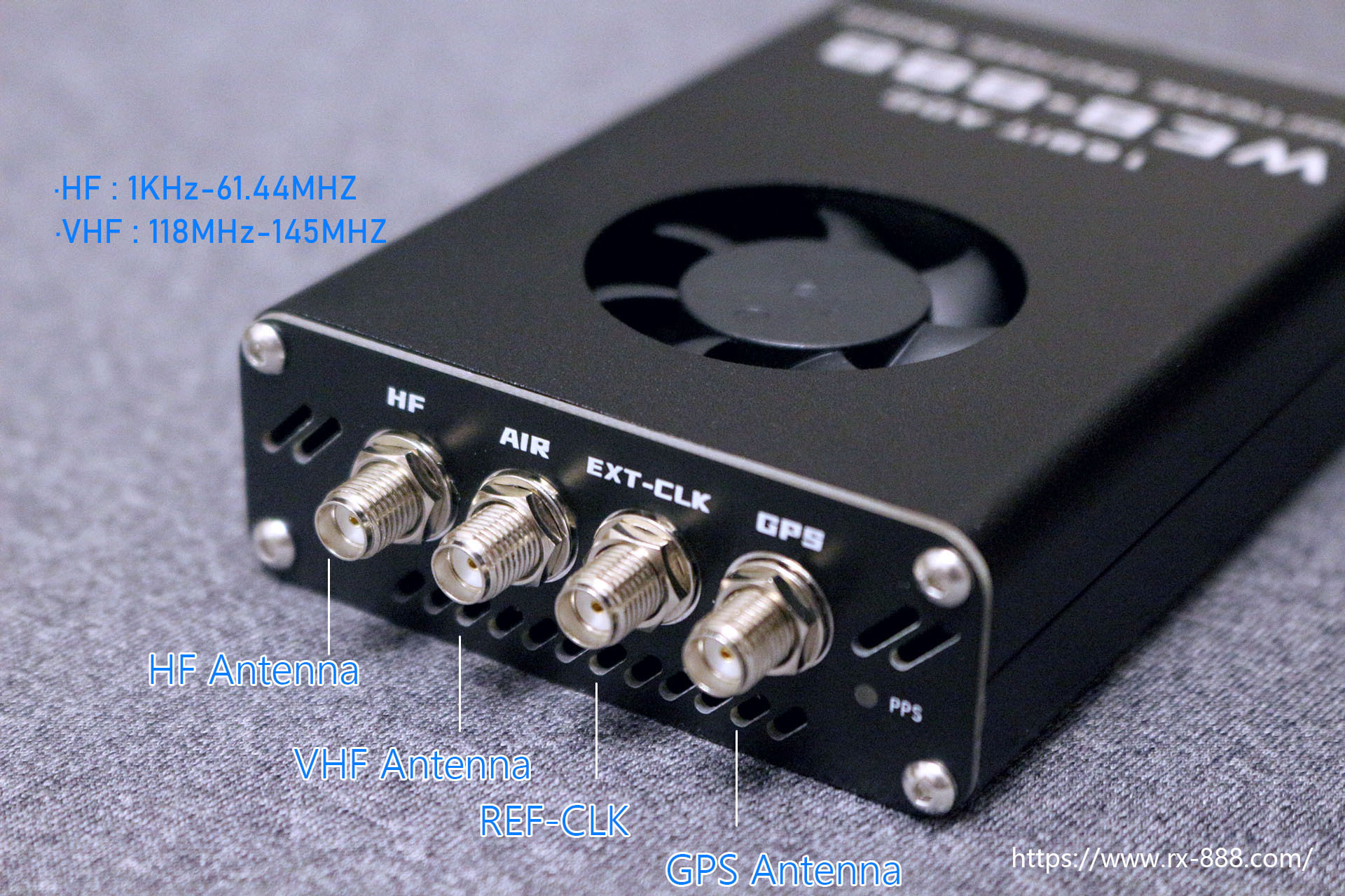
Antennas (Upper Side)
HF Antenna Connected to LNA with a 64MHz LPF.
VHF Antenna Connected to LNA through a BPF centered at 129MHz.
Reference Clock Input Input a 10MHz sine wave or square wave with 0.1-3.0 V peak-to-peak as the reference clock of the Si5351.
GPS Antenna Active GPS antenna with 3.3V bias power supplied.
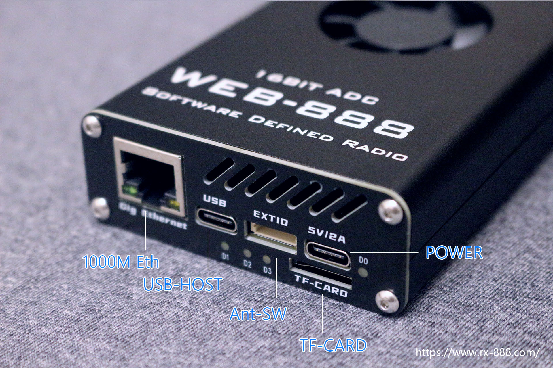
Miscellaneous Connectors (Lower Side)
1000MHz Ethernet Supports 1000MHz or 100MHz Ethernet.
USB Host Plug in USB devices like USB Hub, USB Wi-Fi Dongle, USB UART Dongle, etc.
EXTIO Currently, the interface supports use with Antenna switch extension. The pin definition is shown in the following image. The GND pin is on the TF card side. The connector is SH 1.0, 8 PIN, male connector.
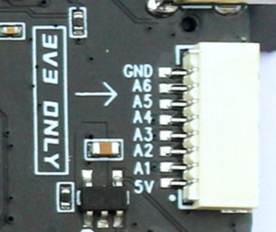
EXTIO Warning
Although the EXTIO connector provides 5V power supply, GPIOs are still 3.3V. All GPIOs are connected directly to the FPGA. Please ensure you have isolation and ESD protection.
USB-C Power Input Ensure you supply a good 5V with 2A or higher.
TF Card Slot TF card (Micro SD card). The card is inserted upside (label side) down.